
SCSI = Small Computer System Interface
SCSI-3 External Hi D-Sub (Differential)
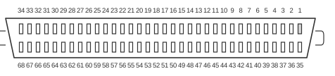 68 pin hi-density D-SUB female connector at the controller and devices.
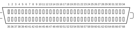 68 pin hi-density D-SUB male connector at the cable.
The 68-pin high-density D-Sub connector (DH68) is the standard external Wide SCSI connector defined in SCSI-2 (ANSI X3.131-1994) and carried forward through the SCSI-3 SPI series (INCITS 253 through INCITS 367-2003), covering transfer rates from Fast-Wide up to Ultra640. This variant uses High Voltage Differential (HVD) signalling, in which each signal is carried as a complementary pair of +/- lines on 5-volt logic, enabling cable runs of up to 25 metres. The HVD electrical variant was formally declared obsolete in SPI-3 (INCITS 336-2000), superseded by Low Voltage Differential (LVD) for new designs, though HVD hardware remained in service in legacy wide-SCSI installations. The connector body has two rows of 34 contacts at 1.27 mm pitch and carries a 16-bit data bus (DB0–DB15) with two parity lines, plus the full set of SCSI bus control signals and termination power.
| Pin | Name | Dir | Description |
|---|---|---|---|
| 1 | +DB12 | IN/OUT | +Data Bus 12 |
| 2 | +DB13 | IN/OUT | +Data Bus 13 |
| 3 | +DB14 | IN/OUT | +Data Bus 14 |
| 4 | +DB15 | IN/OUT | +Data Bus 15 |
| 5 | +DPB1 | IN/OUT | +Data Bus Parity (odd Parity) |
| 6 | GND | - | Ground |
| 7 | +DB0 | IN/OUT | +Data Bus 0 |
| 8 | +DB1 | IN/OUT | +Data Bus 1 |
| 9 | +DB2 | IN/OUT | +Data Bus 2 |
| 10 | +DB3 | IN/OUT | +Data Bus 3 |
| 11 | +DB4 | IN/OUT | +Data Bus 4 |
| 12 | +DB5 | IN/OUT | +Data Bus 5 |
| 13 | +DB6 | IN/OUT | +Data Bus 6 |
| 14 | +DB7 | IN/OUT | +Data Bus 7 |
| 15 | +DPB | IN/OUT | +Data Bus Parity (odd Parity) |
| 16 | DIFFSENSE | ? | ? |
| 17 | TERMPWR | IN/OUT | Termination Power |
| 18 | TERMPWR | IN/OUT | Termination Power |
| 19 | RES | - | Reserved |
| 20 | +ATN | IN | +Attention |
| 21 | GND | - | Ground |
| 22 | +BSY | IN/OUT | +Bus is busy |
| 23 | +ACK | IN | +Acknowledge |
| 24 | +RST | IN/OUT | +Reset |
| 25 | +MSG | OUT | +Message |
| 26 | +SEL | IN/OUT | +Select |
| 27 | +C/D | OUT | +Control or Data |
| 28 | +REQ | OUT | +Request |
| 29 | +I/O | OUT | +In/Out |
| 30 | GND | - | Ground |
| 31 | +DB8 | IN/OUT | +Data Bus 8 |
| 32 | +DB9 | IN/OUT | +Data Bus 9 |
| 33 | +DB10 | IN/OUT | +Data Bus 10 |
| 34 | +DB11 | IN/OUT | +Data Bus 11 |
| 35 | -DB12 | IN/OUT | -Data Bus 12 |
| 36 | -DB13 | IN/OUT | -Data Bus 13 |
| 37 | -DB14 | IN/OUT | -Data Bus 14 |
| 38 | -DB15 | IN/OUT | -Data Bus 15 |
| 39 | -DPB1 | IN/OUT | -Data Bus Parity (odd Parity) |
| 40 | GND | - | Ground |
| 41 | -DB0 | IN/OUT | -Data Bus 0 |
| 42 | -DB1 | IN/OUT | -Data Bus 1 |
| 43 | -DB2 | IN/OUT | -Data Bus 2 |
| 44 | -DB3 | IN/OUT | -Data Bus 3 |
| 45 | -DB4 | IN/OUT | -Data Bus 4 |
| 46 | -DB5 | IN/OUT | -Data Bus 5 |
| 47 | -DB6 | IN/OUT | -Data Bus 6 |
| 48 | -DB7 | IN/OUT | -Data Bus 7 |
| 49 | -DPB | IN/OUT | -Data Bus Parity (odd Parity) |
| 50 | GND | - | Ground |
| 51 | TERMPWR | IN/OUT | Termination Power |
| 52 | TERMPWR | IN/OUT | Termination Power |
| 53 | RES | - | Reserved |
| 54 | -ATN | IN | -Attention |
| 55 | GND | - | Ground |
| 56 | -BSY | IN/OUT | -Bus is busy |
| 57 | -ACK | IN | -Acknowledge |
| 58 | -RST | IN/OUT | -Reset |
| 59 | -MSG | OUT | -Message |
| 60 | -SEL | IN/OUT | -Select |
| 61 | -C/D | OUT | -Control or Data |
| 62 | -REQ | OUT | -Request |
| 63 | -I/O | OUT | -In/Out |
| 64 | GND | - | Ground |
| 65 | -DB8 | IN/OUT | -Data Bus 8 |
| 66 | -DB9 | IN/OUT | -Data Bus 9 |
| 67 | -DB10 | IN/OUT | -Data Bus 10 |
| 68 | -DB11 | IN/OUT | -Data Bus 11 |
Signals
- +DB0 / -DB0 through +DB7 / -DB7 — complementary HVD differential pairs for the lower data byte (bits 0–7); pins 7–14 carry the positive lines and pins 41–48 the negative lines.
- +DB8 / -DB8 through +DB11 / -DB11 — upper data byte bits 8–11; positive lines on pins 31–34, negative on pins 65–68.
- +DB12 / -DB12 through +DB15 / -DB15 — upper data byte bits 12–15; positive lines on pins 1–4, negative on pins 35–38.
- +DPB / -DPB — differential parity pair for the lower byte (DB0–DB7); pins 15 and 49.
- +DPB1 / -DPB1 — differential parity pair for the upper byte (DB8–DB15); pins 5 and 39.
- DIFFSENSE — pin 16; sampled by LVD/MSE multimode devices to detect bus type; not driven by HVD devices. Its direction is undefined in an HVD-only context.
- TERMPWR — termination power supply pins (17, 18, 51, 52); supply regulated voltage to bus terminators.
- RES — reserved pins (19, 53); must not be connected.
- +ATN / -ATN — differential Attention signal; asserted by an initiator to request a Message Out phase.
- +BSY / -BSY — differential Bus Busy; wired-OR across all devices; indicates the bus is in use.
- +ACK / -ACK — differential Acknowledge; handshake response from the initiator during a data transfer.
- +RST / -RST — differential Reset; hard reset of all SCSI devices on the bus when asserted.
- +MSG / -MSG — differential Message; target-driven phase indicator distinguishing message from command/data phases.
- +SEL / -SEL — differential Select; used during selection and reselection phases.
- +C/D / -C/D — differential Control/Data; driven by the target to indicate whether the current phase transfers commands/status (high) or data (low).
- +REQ / -REQ — differential Request; target-driven handshake signal paired with ACK.
- +I/O / -I/O — differential In/Out; driven by the target to indicate transfer direction relative to the initiator.
- GND — signal ground return; distributed across pins 6, 21, 30, 40, 50, 55, 64.
Notes
- Direction is device relative to bus (other devices).
- HVD differential signalling uses complementary +/− line pairs for every signal, providing high noise immunity at 5-volt logic levels and supporting cable lengths up to 25 metres.
- HVD was declared obsolete in SPI-3 (INCITS 336-2000); the maximum bus speed supported by HVD was Ultra (20 MT/sec). LVD (3.3 V) superseded HVD for all new Wide SCSI designs.
- HVD and LVD are electrically incompatible and must never be mixed on the same bus segment; connecting an LVD device to an HVD bus can damage hardware.
- The connector body has two rows of 34 contacts at 1.27 mm pitch. The female (socket) connector is fitted at the controller and devices; the male (plug) connector is at the cable end.
- Exactly two terminators are required per bus segment, fitted at the two extreme ends only. HVD uses passive HVD terminators (differential terminator impedance: 122 ohms); active termination is not used with HVD.
- TERMPWR pins (17, 18, 51, 52) supply power to bus terminators. Multiple TERMPWR pins are provided for redundancy and current capacity.
- The DIFFSENSE pin (pin 16) is not driven by HVD devices but is monitored by any LVD/MSE multimode device that may be attached; its state determines whether the bus operates in LVD or SE mode on a multimode bus.
- All SCSI bus signals in HVD mode are active-low on the positive (+) line of each pair.
References
- 68-Pin SCSI Cable Pinout for SE and HVD Interface
- LVD, SE, HVD SCSI Compatibility — Or Not
- SCSI FAQ Part 4 — Cabling, Termination, and Connector Technical Answers
- SCSI Parallel Interface - 2 (SPI-2) Working Drafts Index
- SCSI Parallel Interface - 5 (SPI-5) Working Drafts Index
- SCSI-2 Specification Section 5: Physical Characteristics (ANSI X3.131-1994 transcription)
- SCSI Revision Levels | Seagate Support