 Apple
Macintosh - Euro-DIN 96-pin Processor-Direct Slot
Apple
Macintosh - Euro-DIN 96-pin Processor-Direct Slot
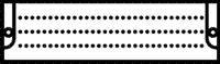
The Euro-DIN 96-pin PDS expansion connector on the main logic board is physically and electrically identical to the 68020 Direct Slot used in the Macintosh LC. This slot provides direct access to all of the 68030/020 data and address signals, and a selection of control signals.
| Pin | Name |
|---|---|
| a1 | GND |
| a2 | +5V |
| a3 | +5V |
| a4 | +5V |
| a5 | /DELAY.CS |
| a6 | /VMA |
| a7 | /BG |
| a8 | /LDS |
| a9 | GND |
| a10 | A2 |
| a11 | A5 |
| a12 | A8 |
| a13 | A11 |
| a14 | A14 |
| a15 | A17 |
| a16 | reserved |
| a17 | n/c |
| a18 | reserved |
| a19 | reserved |
| a20 | D1 |
| a21 | D4 |
| a22 | D7 |
| a23 | D10 |
| a24 | D13 |
| a25 | +5/3.7V |
| a26 | A19 |
| a27 | A22 |
| a28 | FC0 |
| a29 | /IPL0 |
| a30 | /BERR |
| a31 | GND |
| a32 | GND |
| b1 | GND |
| b2 | +5V |
| b3 | +5V |
| b4 | +5V |
| b5 | /SYS.PWR |
| b6 | /BR |
| b7 | /DTACK |
| b8 | /UDS |
| b9 | +5/0V |
| b10 | A3 |
| b11 | A6 |
| b12 | A9 |
| b13 | A12 |
| b14 | A15 |
| b15 | A18 |
| b16 | reserved |
| b17 | reserved |
| b18 | reserved |
| b19 | +12V |
| b20 | D2 |
| b21 | D5 |
| b22 | D8 |
| b23 | D11 |
| b24 | D14 |
| b25 | +5V |
| b26 | A20 |
| b27 | A23 |
| b28 | FC1 |
| b29 | /IPL1 |
| b30 | /EXT.DTACK |
| b31 | 16M |
| b32 | GND |
| c1 | GND |
| c2 | +5V |
| c3 | +5V |
| c4 | +5V |
| c5 | /VPA |
| c6 | /BGACK |
| c7 | R/W |
| c8 | /AS |
| c9 | A1 |
| c10 | A4 |
| c11 | A7 |
| c12 | A10 |
| c13 | A13 |
| c14 | A16 |
| c15 | reserved |
| c16 | n/c |
| c17 | reserved |
| c18 | reserved |
| c19 | D0 |
| c20 | D3 |
| c21 | D6 |
| c22 | D9 |
| c23 | D12 |
| c24 | D15 |
| c25 | GND |
| c26 | A21 |
| c27 | E |
| c28 | FC2 |
| c29 | /IPL2 |
| c30 | /SYS.RST |
| c31 | GND |
| c32 | GND |
Signal Description
- D0-D15: Unbuffered data bus, bits 0 through 15
- A1-A23: Unbuffered address bus, bits 1 through 23
- 16M: 16 MHz clock
- /EXT.DTACK: External data transfer acknowledge. This signal is an input to the processor logic glue. Assertion delays external generation of the /DTACK signal.
- E: E(enable) clock
- /BERR: Bus error signal generated whenever /AS remains low for more than about 250 us.
- /IPL0-/IPL2: Input priority level lines 0 through 2.
- /SYS.RST: Initiates a system reset.
- /SYS.PWR: A signal from the Power Manager indicated that associated circuits should tri-state their outputs and go inte idle state; /SYS.PWR is pulled high (deasserted) during sleep state.
- /AS: Address strobe
- /UDS: Upper data strobe
- /LDS: Lower data strobe
- R/W: Defines bus transfer as read or write signal
- /DTACK: Data transfer acknowledge
- /DELAY.CS: Indicates that a wait state is inserted into the current memory cycle and that you can delay a CS.
- /BG: Bus grant
- /BGACK: Bus grant acknowledge
- /BR: Bus request
- /VMA: Valid memory access
- /VPA: Valid peripheral address
- FC0-FC2: Function code lines 0 through 2
- +5/0V: Provides +5V when the system is running normally and 0V when the system is in sleep mode.
- +5/3.7V: Provides +5V when the system is running normally and 3.7V when the system is in sleep mode.
References
- Macintosh LC II Computer - Developer Note (PDF link)