
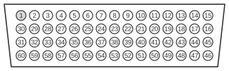
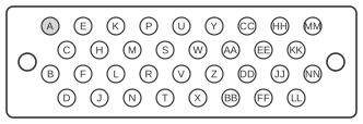
 V.35 DCE Cable Pinout (DB-60 to 34-Pin)
The Cisco V.35 DCE cable (Cisco part numbers CAB-V35FC and CAB-V35MC) connects the proprietary 60-pin DB-60 connector on Cisco 4000, 4500, 4700, 7000, and AGS+ series routers to a 34-pin Winchester (ISO 2593 / MRAC-34) female receptacle at the network end. ITU-T V.35 (October 1984, formally withdrawn but widely adopted as a de facto WAN standard) uses hybrid signalling: balanced differential V.11 pairs carry data and clock signals, whilst V.28 unbalanced circuits handle modem control lines. In DCE mode the Cisco router supplies the transmit and receive clocks (SCT, SCR) to the attached DTE device, and the signal directions on the data pairs are reversed relative to the DTE cable variant. The interface type and DTE/DCE mode are selected on the DB-60 by the mode-shorting pin groups.
| 60 Pin1 | Signal | Description | Direction | 34 Pin | Signal |
|---|---|---|---|---|---|
| J1-49 J1-48 | MODE_1 GND | Shorting group | - | - | - |
| J1-50 J1-51 | MODE_0 GND | Shorting group | - | - | - |
| J1-53 J1-54 J1-55 J1-56 | TxC/NIL RxC_TxCE RxD/TxD GND | Shorting group | - | - | - |
| J1-46 | Shield_GND | Single | - | J2-A | Frame GND |
| J1-45 Shield | Circuit_GND - | Twisted pair no. 12 | - - | J2-B Shield | Circuit GND - |
| J1-35 Shield | CTS/RTS - | Twisted pair no. 8 | ← - | J2-C Shield | RTS - |
| J1-42 Shield | RTS/CTS - | Twisted pair no. 9 | → - | J2-D Shield | CTS - |
| J1-43 Shield | DTR/DSR - | Twisted pair no. 10 | → - | J2-E Shield | DSR - |
| J1-44 Shield | LL/DCD - | Twisted pair no. 11 | → - | J2-F Shield | RLSD - |
| J1-34 Shield | DSR/DTR - | Twisted pair no. 7 | ← - | J2-H Shield | DTR - |
| J1-33 Shield | DCD/LL - | Twisted pair no. 6 | ← - | J2-K Shield | LT - |
| J1-28 J1-27 | RxD/TxD+ RxD/TxD- | Twisted pair no. 5 | ← ← | J2-P J2-S | SD+ SD- |
| J1-18 J1-17 | TxD/RxD+ TxD/RxD- | Twisted pair no. 1 | → → | J2-R J2-T | RD+ RD- |
| J1-26 J1-25 | RxC/TxCE+ RxC/TxCE- | Twisted pair no. 4 | ← ← | J2-U J2-W | SCTE+ SCTE- |
| J1-22 J1-21 | NIL/RxC+ NIL/RxC- | Twisted pair no. 3 | → → | J2-V J2-X | SCR+ SCR- |
| J1-20 J1-19 | TxCE/TxC+ TxCE/TxC- | Twisted pair no. 2 | → → | J2-Y J2-AA | SCT+ SCT- |
Notes
- Arrows indicate signal direction: → indicates DTE to DCE, and ← indicates DCE to DTE.
- (1) Any pin not referenced is not connected.
- The female Winchester receptacle at the network (34-pin) end distinguishes DCE cables from DTE cables, which carry a male Winchester plug.
- Data and clock signals use V.11 balanced differential pairs for noise immunity; modem control signals (RTS, CTS, DTR, DSR, RLSD/DCD, LL) use V.28 single-ended circuits.
- The DB-60 mode-shorting groups (J1-49/48, J1-50/51, J1-53–56) select V.35 interface type and DCE mode; removing the shorting block or fitting a different cable group reverts the port to another standard.
- V.35 is recommended by ITU-T for speeds up to 48 kbit/s, but the interface is commonly operated at 64 kbit/s to 2 Mbit/s on WAN links using HDLC, X.25, PPP, or Frame Relay encapsulations.
Signals
- MODE_1 / GND — DB-60 shorting group (J1-49/48); selects interface type in conjunction with MODE_0.
- MODE_0 / GND — DB-60 shorting group (J1-50/51); selects interface type in conjunction with MODE_1.
- TxC/NIL, RxC_TxCE, RxD/TxD, GND — DB-60 shorting group (J1-53–56); selects DCE mode and clock routing on the port.
- Shield_GND — Frame (chassis) ground; J1-46 to J2-A.
- Circuit_GND — Signal reference ground; J1-45 to J2-B (twisted with shield).
- CTS/RTS — Clear to Send (DCE→DTE); J1-35 to J2-C. V.28 unbalanced. The DCE asserts this to indicate it is ready to accept data from the DTE.
- RTS/CTS — Request to Send (DTE→DCE); J1-42 to J2-D. V.28 unbalanced. The DTE asserts this to request permission to transmit.
- DTR/DSR — Data Terminal Ready (DTE→DCE); J1-43 to J2-E. V.28 unbalanced.
- LL/DCD — Local Loopback / Received Line Signal Detect (DTE→DCE); J1-44 to J2-F (RLSD). V.28 unbalanced.
- DSR/DTR — Data Set Ready (DCE→DTE); J1-34 to J2-H. V.28 unbalanced. The DCE indicates it is powered and ready.
- DCD/LL — Data Carrier Detect / Local Test (DCE→DTE); J1-33 to J2-K (LT). V.28 unbalanced.
- RxD/TxD+ and RxD/TxD− — Receive Data positive/negative (DCE→DTE in DCE mode); J1-28/J1-27 to J2-P/J2-S (SD+/SD−). V.11 balanced differential pair.
- TxD/RxD+ and TxD/RxD− — Transmit Data positive/negative (DTE→DCE in DCE mode); J1-18/J1-17 to J2-R/J2-T (RD+/RD−). V.11 balanced differential pair.
- RxC/TxCE+ and RxC/TxCE− — Receive Clock / Terminal Timing positive/negative; J1-26/J1-25 to J2-U/J2-W (SCTE+/SCTE−). V.11 balanced differential pair.
- NIL/RxC+ and NIL/RxC− — Receive Clock (SCR) positive/negative (DCE→DTE); J1-22/J1-21 to J2-V/J2-X (SCR+/SCR−). V.11 balanced differential pair. The DCE drives this clock for DTE receive timing.
- TxCE/TxC+ and TxCE/TxC− — Send Clock / Transmit Clock (SCT) positive/negative (DCE→DTE); J1-20/J1-19 to J2-Y/J2-AA (SCT+/SCT−). V.11 balanced differential pair. The DCE drives this clock for DTE transmit timing.