
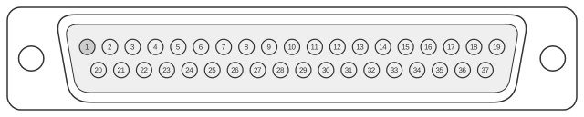
 37 pin D-SUB male connector at the DTE (Computer).
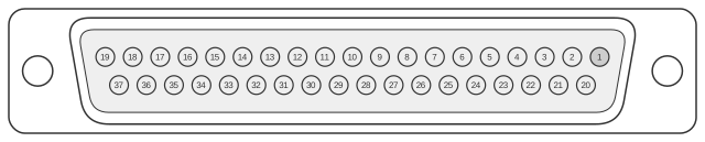 37 pin D-SUB female connector at the DCE (Modem).
TIA/EIA-449 (RS-449), published in 1977, defines the functional and mechanical characteristics of a general-purpose serial interface between data terminal equipment (DTE) and data communications equipment (DCE), using a 37-position D-sub primary connector (ISO 4902) and an optional 9-position D-sub secondary connector for auxiliary circuits. Balanced differential signals follow RS-422 (TIA/EIA-422-B) electrical characteristics, whilst unbalanced signals follow RS-423 (TIA/EIA-423-B); the standard was intended as the successor to RS-232, but the unwieldy 37-pin connector made it impractical and it was superseded by TIA/EIA-530 in 1992, which delivers equivalent functionality via the more compact DB-25 shell. RS-449 remains on legacy telecommunications equipment and references ITU-T V.24 circuit numbers for signal definitions.
| Pin | Name | V.24 | Dir | Description | Type |
|---|---|---|---|---|---|
| 1 | 101 | - | Shield | Ground | |
| 2 | SI | 112 | OUT | Signal Rate Indicator | Control |
| 3 | n/a | n/a | unused | ||
| 4 | SD- | 103 | OUT | Send Data (A) | Data |
| 5 | ST- | 114 | IN | Send Timing (A) | Timing |
| 6 | RD- | 104 | IN | Receive Data (A) | Data |
| 7 | RS- | 105 | OUT | Request To Send (A) | Control |
| 8 | RT- | 115 | IN | Receive Timing (A) | Timing |
| 9 | CS- | 106 | IN | Clear To Send (A) | Control |
| 10 | LL | 141 | OUT | Local Loopback | Control |
| 11 | DM- | 107 | IN | Data Mode (A) | Control |
| 12 | TR- | 108.2 | OUT | Terminal Ready (A) | Control |
| 13 | RR- | 109 | IN | Receiver Ready (A) | Control |
| 14 | RL | 140 | OUT | Remote Loopback | Control |
| 15 | IC | 125 | IN | Incoming Call | Control |
| 16 | SF/SR+ | 126 | IN/OUT | Signal Freq./Sig. Rate Select. | Control |
| 17 | TT- | 113 | OUT | Terminal Timing (A) | Timing |
| 18 | TM- | 142 | IN | Test Mode (A) | Control |
| 19 | SG | 102 | - | Signal Ground | Ground |
| 20 | RC | 102b | - | Receive Common | Ground |
| 21 | n/a | n/a | unused | ||
| 22 | SD+ | 103 | OUT | Send Data (B) | Data |
| 23 | ST+ | 114 | IN | Send Timing (B) | Timing |
| 24 | RD+ | 104 | IN | Receive Data (B) | Data |
| 25 | RS+ | 105 | OUT | Request To Send (B) | Control |
| 26 | RT+ | 115 | IN | Receive Timing (B) | Timing |
| 27 | CS+ | 106 | IN | Clear To Send (B) | Control |
| 28 | IS | n/a | OUT | Terminal In Service | Control |
| 29 | DM+ | 107 | IN | Data Mode (B) | Control |
| 30 | TR+ | 108.2 | OUT | Terminal Ready (B) | Control |
| 31 | RR+ | 109 | IN | Receiver Ready (B) | Control |
| 32 | SS | 116 | IN | Select Standby | Control |
| 33 | SQ | 110 | IN | Signal Quality | Control |
| 34 | NS | n/a | OUT | New Signal | Control |
| 35 | TT+ | 113 | OUT | Terminal Timing (B) | Timing |
| 36 | SB | 117 | IN | Standby Indicator | Control |
| 37 | SC | 102a | - | Send Common | Ground |
Signals
| Name | Description | Function |
|---|---|---|
| AA | Shield Ground | Also known as protective ground. This is the chassis ground connection between DTE and DCE. |
| AB | Signal Ground | The reference ground between a DTE and a DCE. Has the value 0 Vdc. |
| BA | Transmitted Data | Data send by the DTE. |
| BB | Received Data | Data received by the DTE. |
| CA | Request To Send | Originated by the DTE to initiate transmission by the DCE. |
| CB | Clear To Send | Send by the DCE as a reply on the RTS after a delay in ms, which gives the DCEs enough time to energize their circuits and synchronize on basic modulation patterns. |
| CC | DCE Ready | Known as DSR. Originated by the DCE indicating that it is basically operating (power on, and in functional mode). |
| CD | DTE Ready | Known as DTR. Originated by the DTE to instruct the DCE to setup a connection. Actually it means that the DTE is up and running and ready to communicate. |
| CE | Ring Indicator | A signal from the DCE to the DTE that there is an incoming call (telephone is ringing). Only used on switched circuit connections. |
| CF | Received Line Signal Detector | Known as DCD. A signal send from DCE to its DTE to indicate that it has received a basic carrier signal from a (remote) DCE. |
| CH/CI | Data Signal Rate Select (DTE/DCE Source> | A control signal that can be used to change the transmission speed. |
| DA | Transmit Signal Element Timing (DTE Source) | Timing signals used by the DTE for transmission, where the clock is originated by the DTE and the DCE is the slave. |
| DB | Transmitter Signal Element Timing (DCE Source) | Timing signals used by the DTE for transmission. |
| DD | Receiver Signal Element Timing (DCE Source) | Timing signals used by the DTE when receiving data. |
| IS | terminal In Service | Signal that indicates that the DTE is available for operation |
| NS | New Signal | A control signal from the DTE to the DCE. It instructs the DCE to rapidly get ready to receive a new analog signal. It helps master-station modems rapidly synchronize on a new modem at a tributary station in multipoint circuits |
| RC | Receive Common | A signal return for receiver circuit reference |
| LL | Local Loopback / Quality Detector | A control signal from the DTE to the DCE that causes the analog transmission output to be connected to the analog receiver input. |
| RL | Remote Loopback | Signal from the DTE to the DCE. The local DCE then signals the remote DCE to loopback the analog signal and thus causing a line loopback. |
| SB | Standby Indicator | Signal from the DCE to indicate if it is uses the normal communication or standby channel |
| SC | Send Common | A return signal for transmitter circuit reference |
| SF | Select Frequency | A signal from the DTE to tell the DCE which of the two analog carrier frequencies should be used. |
| SS | Select Standby | A signal from DTE to DCE, to switch between normal communication or standby channel. |
| TM | Test Mode | A signal from the DCE to the DTE that it is in test-mode and can’t send any data. |
| Reserved for Testing |
Notes
- The 37-pin primary connector carries the main data, timing, and control circuits; an optional 9-pin secondary connector (DE-9) accommodates auxiliary or secondary-channel circuits.
- Balanced differential pairs (RS-422) are wired A (pins 4–18, odd side) and B (pins 22–37, even side). Wire A must connect to A and wire B to B — crossing the wires inverts data or clock polarity.
- RS-422 balanced circuits: minimum 2 V differential output across a 100 Ω load; receiver sensitivity ±200 mV; common-mode range −7 V to +7 V; maximum data rate 10 Mbit/s; cable up to approximately 1200 m at low data rates.
- RS-423 unbalanced circuits (control signals): maximum driver output ±6 V; receiver sensitivity ±200 mV; maximum data rate 100 kbit/s.
- Circuit numbers in the V.24 column correspond to ITU-T V.24 (02/2000) interchange circuit definitions; for example, circuit 103 = Transmitted Data, 104 = Received Data, 105 = Request to Send, 106 = Ready for Sending.
- EIA-449-1 (1980 addendum) incorporated RS-422-A and RS-423-A electrical specifications. The standard was rescinded in January 1986 and formally superseded by EIA/TIA-530-A, which provides equivalent functionality using the smaller DB-25 connector.
- Pins 3 and 21 are unused in the primary connector.
References
- AN-1031: TIA/EIA-422-B Overview — Texas Instruments, RS-422 differential electrical specifications
- AN-917: Popular Connector Pin Assignments for Data Communications — Texas Instruments, RS-449 DB-37 and companion connector pinout reference
- Overview of Serial Communication Standards — Sealevel Systems, comparative RS-232/RS-422/RS-423/RS-449/RS-530 overview
- ITU-T Recommendation V.24: List of Definitions for Interchange Circuits — International Telecommunication Union, circuit number definitions used in RS-449 pin table