
ITU-TSS (CCITT) X.21 is also known as ISO 4903
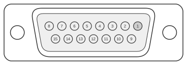 15 pin D-SUB female connector at the DTE (Computer).
15 pin D-SUB female connector at the DCE (Modem).
ITU-T Recommendation X.21 (09/92) defines a synchronous serial interface between Data Terminal Equipment (DTE) and Data Circuit-terminating Equipment (DCE) for operation on public circuit-switched data networks, first recommended by CCITT in 1976. The interface uses a 15-pin DA-15 (DB-15) sub-D connector as specified by ISO 4903, with eight primary signal types: Transmit (T), Receive (R), Control (C), Indication (I), Signal Element Timing (S), Byte Timing (B), Signal Ground (G), and DTE Common Return (Ga). Balanced circuits use V.11 (X.27) differential signalling, capable of data rates from 600 bps to 64 kbps on subscriber networks and up to 10 Mbps electrically; unbalanced circuits use V.10 (X.26) and are employed only at lower rates below 9600 bps. Because the clock is DCE-supplied, X.21 is inherently synchronous, and hardware handshaking is performed via the Control (DTE-to-DCE) and Indication (DCE-to-DTE) circuits rather than the numerous control lines found in RS-232/V.24 interfaces.
Pinout for balanced X.21 (according to ISO4903)
| Pin | Name | DTE I/O | Description | Type |
|---|---|---|---|---|
| 1 | Shield | - | Shield | Ground |
| 2 | T (A) | OUT | Transmit (A) | Data |
| 3 | C (A) | OUT | Control (A) | Control |
| 4 | R (A) | IN | Receive (A) | Data |
| 5 | I (A) | IN | Indication (A) | Control |
| 6 | S (A) | IN | Signal Timing (A) | Timing |
| 7 | B (A) / unused | IN | Byte Timing (A) or unassigned | Timing |
| 8 | G | - | Ground | Ground |
| 9 | T (B) | OUT | Transmit (B) | Data |
| 10 | C (B) | OUT | Control (B) | Control |
| 11 | R (B) | IN | Receive (B) | Data |
| 12 | I (B) | IN | Indication (B) | Control |
| 13 | S (B) | IN | Signal Timing (B) | Timing |
| 14 | B (B) / unused | IN | Byte Timing (B) or unassigned | Timing |
| 15 | unused |
Notes
The physical interface between the DTE and the locally supplied DCE is defined in ITU-T Recommendation X.21. Balanced circuits (V.11/X.27) use differential signalling equivalent to RS-422, with a minimum differential output of 0.55 V across a 100 Ω load; unbalanced circuits (V.10/X.26) are used only below 9600 bps. Above 9600 bps, V.11 balanced circuits are required. Pin 15 is unused and carries no assignment in the standard. Byte Timing (B, pins 7/14) is optional and frequently left unconnected; where used, it provides 8-bit byte-boundary timing to align call-control characters during the call-control phase.
A companion standard, X.21bis, was defined for use on existing analogue networks; it is a subset of EIA-232D/V.24, allowing legacy equipment to be interfaced without a native X.21 DCE.
Signals
- Shield — Protective earth/shield connection; may be connected to chassis ground.
- G (Signal Ground) — Provides the voltage reference for all logic states on other circuits; may be bonded to protective ground.
- Ga (DTE Common Return) — Used only in unbalanced (V.10/X.26) configurations; provides the reference return for DCE receivers. Carried on pin 8 in the DA-15 connector.
- T (Transmit, A/B) — Balanced pair carrying binary data from DTE to DCE; used both during the data-transfer phase and during call-control phases (call connect or call disconnect).
- C (Control, A/B) — DTE-to-DCE control circuit; must be ON during the data-transfer phase and may be ON or OFF during call-control phases as defined by the X.21 protocol.
- R (Receive, A/B) — Balanced pair carrying binary data from DCE to DTE.
- I (Indication, A/B) — DCE-to-DTE control circuit; indicates to the DTE the type of data being sent on the Receive circuit. Must be ON during the data-transfer phase; may vary during call-control phases.
- S (Signal Element Timing, A/B) — Clock signal supplied by the DCE; provides the DTE and DCE with sampling timing for the Transmit and Receive circuits respectively. Always ON during active operation.
- B (Byte Timing, A/B) — Optional 8-bit byte-boundary timing circuit; normally ON, transitioning to OFF at the last bit of each 8-bit byte on the S clock. Frequently unused (pins 7 and 14).
X.21 cross-cable scheme
| X.21 | X.21 |
|---|---|
| 1 | 1 |
| 2 | 4 |
| 3 | 5 |
| 4 | 2 |
| 5 | 3 |
| 6 | 7 |
| 7 | 6 |
| 8 | 8 |
| 9 | 11 |
| 10 | 12 |
| 11 | 9 |
| 12 | 10 |
| 13 | 14 |
| 14 | 13 |
| 15 |