
 34 pin M/34 male connector.
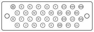 34 pin M/34 female connector.
ITU-T Recommendation V.35 (1984, formally withdrawn) originally specified data transmission at 48 kbit/s over 60–108 kHz group-band circuits, but in practice the interface evolved into a widely used WAN serial standard supporting rates from 56 kbit/s up to T1/E1 and beyond. It is identified by its distinctive 34-pin Winchester (M/34) connector and combines V.11 balanced differential signalling for data and clock circuits with V.28 unbalanced signalling for control circuits. The functional interchange circuits follow ITU-T V.24 definitions. Despite the standard’s formal withdrawal — with V.36 and V.37 cited as alternatives — the V.35 connector and interface naming persisted across decades of router, CSU/DSU, and WAN equipment from major vendors.
| Pin | Name | Dir | Description |
|---|---|---|---|
| A | - | Chassis Ground | |
| B | - | Signal Ground | |
| C | RTS | OUT | Request To Send |
| D | CTS | IN | Clear To Send |
| E | DSR | IN | Data Set Ready |
| F | DCD | IN | Data Carrier Detect |
| H | DTR | OUT | Data Terminal Ready |
| J | LL | IN | Local Loopback |
| K | OUT | Local Test | |
| L | unused | ||
| M | unused | ||
| N | unused | ||
| P | TxD- | OUT | Send Data A |
| R | RxD- | IN | Receive Data A |
| S | TxD+ | OUT | Send Data B |
| T | RxD+ | IN | Receive Data B |
| U | OUT | Terminal Timing A | |
| V | IN | Receive Timing A | |
| W | OUT | Terminal Timing B | |
| X | IN | Receive Timing B | |
| Y | IN | Send Timing A | |
| Z | unused | ||
| AA | IN | Send Timing B | |
| BB | unused | ||
| CC | unused | ||
| DD | unused | ||
| EE | unused | ||
| FF | unused | ||
| HH | unused | ||
| JJ | unused | ||
| KK | unused | ||
| LL | unused | ||
| MM | unused | ||
| NN | unused |
Signals
- A (Chassis Ground) — protective earth connection; not an interchange circuit.
- B (Signal Ground) — reference ground for all unbalanced (V.28) control signals (V.24 circuit 102).
- RTS — Request To Send; DTE asserts to request permission to transmit (V.24 circuit 105); uses V.28 unbalanced signalling.
- CTS — Clear To Send; DCE asserts in response to RTS to indicate the DTE may transmit (V.24 circuit 106); V.28 unbalanced.
- DSR — Data Set Ready; DCE indicates it is connected and ready to operate (V.24 circuit 107); V.28 unbalanced.
- DCD — Data Carrier Detect; DCE indicates a valid carrier has been detected on the line (V.24 circuit 109); V.28 unbalanced.
- DTR — Data Terminal Ready; DTE signals that it is ready for connection (V.24 circuit 108); V.28 unbalanced.
- LL — Local Loopback; loops the local DCE transmitter back to its own receiver for testing; V.28 unbalanced.
- K (Local Test) — indicates that a local loopback test is in progress.
- TxD- / TxD+ (pins P and S) — Transmitted Data, A and B legs of the balanced differential pair; uses V.11 signalling; nominal differential voltage 0.55 V ±20% across a 100 Ω load.
- RxD- / RxD+ (pins R and T) — Received Data, A and B legs of the balanced differential receive pair; V.11 signalling.
- Terminal Timing A/B (pins U and W) — DTE-sourced transmit clock, differential pair; synchronises the DCE to the DTE’s internal clock (V.24 circuit 113).
- Receive Timing A/B (pins V and X) — DCE-sourced receive clock, differential pair; clocks received data into the DTE (V.24 circuit 115).
- Send Timing A/B (pins Y and AA) — DCE-sourced transmit clock, differential pair; clocks transmitted data from the DTE (V.24 circuit 114).
- Unused pins (L, M, N, Z, BB–NN) — not assigned in common V.35 implementations; left unconnected.
Notes
- The M/34 Winchester connector is the industry-standard mechanical form for V.35, though ITU-T V.35 itself did not originally define this connector — it became the de facto standard through vendor adoption.
- V.35 uses a mixed signalling scheme: data and clock circuits (TxD, RxD, Terminal Timing, Receive Timing, Send Timing) use ITU-T V.11 (X.27) balanced differential signalling, whilst control circuits (RTS, CTS, DSR, DCD, DTR, LL) use ITU-T V.28 unbalanced signalling — the same electrical standard as RS-232 control signals.
- Cable should be balanced multipair with a characteristic impedance of 80–120 Ω. Nominal differential signal voltage on data/clock pairs is 0.55 V ±20% with a 100 Ω load. Maximum cable distance is approximately 1200 m (4000 ft) at data rates up to 100 kbit/s.
- Two wiring variants exist in the field: V.35 Winchester and V.35 Straight. These are mirrored with respect to one another — for example, 3Com documented that their Access Builder 4000 V.35 card used the Straight variant, whilst the Dutch PTT supplied a Winchester-pinned interface. Connecting the two variants requires a crossed cable.
- Pin identifiers use letters (A, B, C…) rather than numbers, and skip letters I, O, and Q to avoid confusion with digits. Two-letter identifiers (AA, BB, etc.) follow the single-letter set.
- Transmission is synchronous; all three clock pairs (Terminal Timing, Receive Timing, Send Timing) enable the DTE and DCE to maintain bit-level synchronisation without a separate timing channel.
- ITU-T formally withdrew Recommendation V.35 because the content was considered out of date; ITU-T V.36 and V.37 are cited as the intended successors, though neither displaced the V.35 connector in the market.
References
- ITU-T Recommendation V.35: Data Transmission at 48 kbit/s Using 60–108 kHz Group Band Circuits — ITU-T (withdrawn 1984; governing standard)
- ITU-T Recommendation V.24: List of Definitions for Interchange Circuits Between DTE and DCE — ITU-T (defines functional circuits referenced by V.35)
- ITU-T Recommendation V.28: Electrical Characteristics for Unbalanced Double-Current Interchange Circuits — ITU-T (defines V.28 unbalanced signalling used for V.35 control signals)