
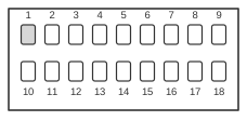
 18 Pin xD-Picture Card Connector
The xD-Picture Card (xD standing for extreme Digital) is a compact flash memory card developed jointly by Olympus and Fujifilm and announced in July 2002. It uses an 18-contact, single-row connector at 1 mm pitch and presents a raw, controllerless NAND flash interface to the host, meaning the host device is responsible for ECC, bad-block management, and wear levelling. Cards were manufactured by Toshiba and Samsung in capacities ranging from 16 MB to 2 GB. The format is proprietary; Olympus and Fujifilm licensed specifications under NDA with no public standards body, and it has since been superseded by SD.
| Pin | Name | Dir | description |
|---|---|---|---|
| 1 | XD_CD# | - | presence detect |
| 2 | R/B# | OUT | Ready / Busy (open-drain) |
| 3 | RE# | IN | Read Enable |
| 4 | CE# | IN | Card Enable |
| 5 | CLE | IN | Command Latch Enable |
| 6 | ALE# | IN | Address Latch Enable |
| 7 | WE# | IN | Write Enable |
| 8 | WP# | IN | Write Protect |
| 9 | GND | - | Ground |
| 10 | SD0 | IN/OUT | data bit 0 |
| 11 | SD1 | IN/OUT | data bit 1 |
| 12 | SD2 | IN/OUT | data bit 2 |
| 13 | SD3 | IN/OUT | data bit 3 |
| 14 | SD4 | IN/OUT | data bit 4 |
| 15 | SD5 | IN/OUT | data bit 5 |
| 16 | SD6 | IN/OUT | data bit 6 |
| 17 | SD7 | IN/OUT | data bit 7 |
| 18 | VCC | - | 3.3V power |
Notes
The card body measures 20 mm × 25 mm × 1.7 mm and weighs approximately 2 g. All 18 contacts are gold-plated and arranged in a single row at 1 mm pitch. Supply voltage is 3.3 V only; the format does not support a 5 V variant. Because the card contains no onboard controller, it exposes a bare NAND flash die interface similar to a TSOP-48 packaged device — the host must issue raw NAND commands and handle ECC correction and bad-block tables.
Signals
- XD_CD# — card-detect signal; pulled low by the card when inserted, allowing the host to sense presence
- R/B# — Ready/Busy; open-drain output from the card indicating whether an internal operation (programme, erase, or read) is in progress (low = busy)
- RE# — Read Enable; host asserts low to clock data out of the card onto the SD0–SD7 bus
- CE# — Card Enable (chip enable); host asserts low to select the card
- CLE — Command Latch Enable; host drives high when the data bus carries a NAND command byte
- ALE# — Address Latch Enable; host drives high when the data bus carries an address byte
- WE# — Write Enable; host asserts low to clock data, commands, or addresses into the card
- WP# — Write Protect; host drives low to inhibit programme and erase operations
- GND — ground reference (pin 9)
- SD0–SD7 — 8-bit bidirectional data bus carrying data, command bytes, and address bytes multiplexed under CLE/ALE# control
- VCC — 3.3 V power supply (pin 18)