
Pin assignment of 5V and 3.3V SmartMedia™
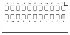 Smartmedia Connector
SmartMedia, formally the Solid State Floppy Disk Card (SSFDC), is a removable NAND flash memory card format created by Toshiba and introduced in 1995. It uses a 22-contact edge connector exposing a raw 8-bit parallel NAND flash bus directly — with no onboard controller — so the host device must manage wear levelling, ECC, and bad-block handling. Two electrically incompatible voltage variants were produced (5 V and 3.3 V), distinguished by the position of a corner notch on the card body. The SSFDC Forum, founded in April 1996, governed the Physical, Electrical, and Logical Format Specifications; the forum wound up in May 2007 as the format was superseded by more capable cards.
| PIN | Name |
|---|---|
| 1 | Vss |
| 2 | CLE |
| 3 | ALE |
| 4 | WE |
| 5 | WP |
| 6 | I/O1 |
| 7 | I/O2 |
| 8 | I/O3 |
| 9 | I/O4 |
| 10 | Vss |
| 11 | Vss |
| 12 | Vcc |
| 13 | I/O5 |
| 14 | I/O6 |
| 15 | I/O7 |
| 16 | I/O8 |
| 17 | Power Detect Vcc |
| 18 | GND (opional on 32Mbit) |
| 19 | R/B |
| 20 | RE |
| 21 | CE |
| 22 | Vcc |
Signals
- Vss — Ground return (pins 1, 10, 11).
- CLE — Command Latch Enable; when high, data on I/O bus is interpreted as a command cycle.
- ALE — Address Latch Enable; when high, data on I/O bus is interpreted as an address cycle.
- WE — Write Enable (active low); latches commands, addresses, and data on its rising edge.
- WP — Write Protect (active low); disables write and erase operations when asserted.
- I/O1–I/O8 — Bidirectional 8-bit parallel data bus carrying commands, addresses, and data.
- Vcc — Supply voltage (pins 12 and 22); 4.5–5.5 V on 5 V cards, 3.0–3.6 V on 3.3 V cards.
- Power Detect Vcc — Voltage detect pin (pin 17) used by the host to sense card presence and voltage variant.
- GND — Additional ground (pin 18); optional on 32 Mbit cards per the electrical specification.
- R/B — Ready/Busy (open-drain output); low while the card is executing an internal operation; returns high when ready.
- RE — Read Enable (active low); clocks data from the card onto the I/O bus.
- CE — Chip Enable (active low); selects the card for communication.
Notes
- The card measures 45 mm × 37 mm × 0.76 mm, making it one of the thinnest removable flash formats produced.
- The 5 V and 3.3 V variants are physically keyed by a corner notch in different positions; a host must read the Power Detect pin (pin 17) to confirm voltage compatibility before operation.
- Maximum data transfer rate is 2 MB/s.
- Capacity ranged from 512 KB to 128 MB; a 256 MB variant was defined but never manufactured.
- Because the interface exposes raw NAND flash with no controller, the host is solely responsible for ECC correction, wear levelling, and bad-block management.
- Card logical organisation follows the FAT file system mapping defined in the SSFDC Logical Format Specification, with block addressing and spare-area ECC layout defined in the same document.
References
- SmartMedia Physical Format Specifications, Web-Online Version 1.00 — SSFDC Forum Technical Committee, 1999
- SmartMedia Electrical Specifications, Web-Online Version 1.00 — SSFDC Forum Technical Committee, 1999
- SmartMedia Logical Format Specifications, Web-Online Version 1.00 — SSFDC Forum Technical Committee, 1999