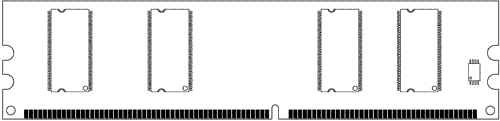
 184-pin DDR SDRAM DIMM
- DIMM: Dual Inline Memory Module
- SDRAM: Synchronous Dynamic Random Access Memory, Synchronous to Positive Clock Edge.
- DDR: Double Data Rate
184-pin DDR DIMMs use two notches on each side to enable compatibility with both low- and highprofile latched sockets. Note that the key position is offset with respect to the center of the DIMM to prevent inserting it backward in the socket. The key notch is positioned to the left, centered, or to the right of the area between pins 52 and 53. This is used to indicate the I/O voltage for the DDR DIMM and to prevent installing the wrong type into a socket that might damage the DIMM.
PIN CONFIGURATIONS (Front side / back side)
| PIN | FRONT | PIN | FRONT | PIN | FRONT | PIN | BACK | PIN | BACK | PIN | BACK |
|---|---|---|---|---|---|---|---|---|---|---|---|
| 1 | VREF | 32 | A5 | 62 | VDD | 93 | VSS | 124 | VSS | 154 | RAS# |
| 2 | DQ0 | 33 | DQ24 | 63 | WE# | 94 | DQ4 | 125 | A6 | 155 | DQ45 |
| 3 | VSS | 34 | VSS | 64 | DQ41 | 95 | DQ5 | 126 | DQ28 | 156 | VDD |
| 4 | DQ1 | 35 | DQ25 | 65 | CAS# | 96 | VDD | 127 | DQ29 | 157 | S0# |
| 5 | DQS0 | 36 | DQS3 | 66 | VSS | 97 | DQS9 | 128 | VDD | 158 | S1# |
| 6 | DQ2 | 37 | A4 | 67 | DQS5 | 98 | DQ6 | 129 | DQS12 | 159 | DQS14 |
| 7 | VDD | 38 | VDD | 68 | DQ42 | 99 | DQ7 | 130 | A3 | 160 | VSS |
| 8 | DQ3 | 39 | DQ26 | 69 | DQ43 | 100 | VSS | 131 | DQ30 | 161 | DQ46 |
| 9 | NC | 40 | DQ27 | 70 | VDD | 101 | NC | 132 | VSS | 162 | DQ47 |
| 10 | NC | 41 | A2 | 71 | NC | 102 | NC | 133 | DQ31 | 163 | NC |
| 11 | VSS | 42 | VSS | 72 | DQ48 | 103 | NC | 134 | CB4 | 164 | VDD |
| 12 | DQ8 | 43 | A1 | 73 | DQ49 | 104 | VDD | 135 | CB5 | 165 | DQ52 |
| 13 | DQ9 | 44 | CB0 | 74 | VSS | 105 | DQ12 | 136 | VDD | 166 | DQ53 |
| 14 | DQS1 | 45 | CB1 | 75 | CK2# | 106 | DQ13 | 137 | CK0 | 167 | NC |
| 15 | VDD | 46 | VDD | 76 | CK2 | 107 | DQS10 | 138 | CKO# | 168 | VDD |
| 16 | CK | 47 | DQS8 | 77 | VDD | 108 | VDD | 139 | VSS | 169 | DQS15 |
| 17 | CK1# | 48 | A0 | 78 | DQS6 | 109 | DQ14 | 140 | DQS17 | 170 | DQ54 |
| 18 | VSS | 49 | CB2 | 79 | DQ50 | 110 | DQ15 | 141 | A10 | 171 | DQ55 |
| 19 | DQ10 | 50 | VSS | 80 | DQ51 | 111 | CKE1 | 142 | CB6 | 172 | VDD |
| 20 | DQ11 | 51 | CB3 | 81 | VSS | 112 | VDD | 143 | VDD | 173 | NC |
| 21 | CKE0 | 52 | BA1 | 82 | NC | 113 | NC | 144 | CB7 | 174 | DQ60 |
| 22 | VDD | KEY | 83 | DQ56 | 114 | DQ20 | KEY | 175 | DQ61 | ||
| 23 | DQ16 | 53 | DQ32 | 84 | DQ57 | 115 | A12 | 145 | VSS | 176 | VSS |
| 24 | DQ17 | 54 | VDD | 85 | VDD | 116 | VSS | 146 | DQ36 | 177 | DQS16 |
| 25 | DQS2 | 55 | DQ33 | 86 | DQS7 | 117 | DQ21 | 147 | DQ37 | 178 | DQ62 |
| 26 | VSS | 56 | DQS4 | 87 | DQ58 | 118 | A11 | 148 | VDD | 179 | DQ63 |
| 27 | A9 | 57 | DQ34 | 88 | DQ59 | 119 | DQS11 | 149 | DQS13 | 180 | VDD |
| 28 | DQ18 | 58 | VSS | 89 | VSS | 120 | VDD | 150 | DQ38 | 181 | SA0 |
| 29 | A7 | 59 | BA0 | 90 | NC | 121 | DQ22 | 151 | DQ39 | 182 | SA1 |
| 30 | VDD | 60 | DQ35 | 91 | SDA | 122 | A8 | 152 | VSS | 183 | SA2 |
| 31 | DQ19 | 61 | DQ40 | 92 | SCL | 123 | DQ23 | 153 | DQ44 | 184 | VDDSPD |
PIN DESCRIPTION
| PIN | NAME FUNCTION |
|---|---|
| A0-A11 | Address input (Multiplexed) |
| BA0~BA1 | Bank Select Address |
| DQ0~Q63 | Data input/output |
| DQ0~DQS7 | Data Strobe input/output |
| CK0, CK0#, CK1, CK1#, CK2, CK2# | Clock input |
| CKE0, CKE1 | Clock enable input |
| S0#, S1# | Chip select input |
| RAS | Row address strobe |
| CAS | Column address strobe |
| WE | Write enable |
| WP | Write protect |
| VDD | Power supply (2.5v) |
| VDDQ | Power supply for DQS (2.5V) |
| VSS | Ground |
| VREF | Power supply for reference |
| VDDSPD | Serial EEPROM Power Supply (2.3V to 3.6V) |
| SDA | Serial data I/O |
| SCL | Serial Clock |
| SA0-SA2 | Address in EEPROM |
| VDDID | VDD identification flag |
| NC | No connection |