
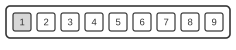
This page documents the connectors used by third-party data and synchronisation cables for the Nokia 5100 mobile phone. The pin layout is specific to this handset and its connector family. Only the pins utilised by the cable or internal interface are listed below.
| Pin | Signal |
|---|---|
| 1 | Gnd |
| 2 | MBus |
| 3 | Vpp |
| 4 | FBus Rx |
| 5 | FBus Tx |
| 7 | Gnd |
| 8 | BSI |
| 9 | VBatt |
Display Connector

| Pin | Signal |
|---|---|
| 1 | LCDRSTX - Reset (2,8V) |
| 2 | VOUT - DC/DC voltage converter output (0V) |
| 3 | UDGND - Gnd (0V) |
| 4 | OSC - External clock (2,8V) |
| 5 | LCDCSX - Chip select input (2,8V) |
| 6 | LCDCDX - Control/display data flag input (2,8V) |
| 7 | SDA - Serial data input (0V) |
| 8 | SCLK - Serial clock input (0V) |
| 9 | VL - Supply voltage (2,8V) |

| Pin | Signal |
|---|---|
| 1 | ROW0 - Keyboard matrix row 0 |
| 2 | ROW1 - Keyboard matrix row 1 |
| 3 | ROW2 - Keyboard matrix row 2 |
| 4 | ROW3 - Keyboard matrix row 3 |
| 5 | ROW4 - Keyboard matrix row 4 |
| 6 | COL0 - keyboard matrix column 0 (flip identification) |
| 7 | COL1 - keyboard matrix column 1 |
| 8 | COL2 - keyboard matrix column 2 |
| 9 | COL3 - keyboard matrix column 3 |
| 10 | COL4 - keyboard matrix column 4 |
| 11 | Signal1 - flip interrupt (not used) |
| 12 | VF |
| 13 | VF |
| 14 | VBATT - Battery Voltage |
| 15 | UAGND - Analog Gnd |
| 16 | PWRON - Power On key |
| 17 | LCDCDX - LCD driver code/data selection |
| 18 | SCLK - LCD driver serial clock |
| 19 | SDA - LCD driver serial data |
| 20 | LCDCSX - LCD driver chip select |
| 21 | LCDRSTX - LCD driver reset |
| 22 | UDGND - Digital Gnd |
| 23 | BUZZER - Buzzer PWM control |
| 24 | VL - Supply voltage |
| 25 | SPARE - Call indicator LED |
| 26 | LIGHT - Illumination control |
| 27 | EARN - Speaker neutral |
| 28 | EARP - Speaker positive |
Notes
Pin numbers refer to the connector on the handset; pins not listed are unused by the cable.
References
- Nokia 5100 Service Manual (NPM-6/NPM-6X) — System Module / System Connector — Nokia Corporation.