
hard disks cables wiring  40 pin IDC female connector to the cable
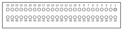 50 pin CompactFlash female connector to the cable
A CF-to-IDE adapter allows a CompactFlash card to be used in place of a conventional ATA (IDE) hard disc by connecting the card’s 50-pin socket (two rows of 25 contacts on 1.27 mm centres) to a standard 40-pin IDC host connector. When CF pin 9 (-OE) is tied to ground at power-up, the card enters True IDE Mode and presents itself to the host as a standard ATA storage device, as defined in the CF+ and CompactFlash Specification Rev. 1.4 (CompactFlash Association, 1999). The adapter is entirely passive for the data, address, and control lines; only the power rail (Vcc) and a current-limiting resistor for the activity LED require additional connections.
| IDE-Signal | IDE-Pin | Connect to | CF-Signal | CF-Pin | CF-Pin | CF-Signal | Connect to | IDE-Pin | IDE-Signal |
|---|---|---|---|---|---|---|---|---|---|
| - | - | GND | GND | 1 | 26 | -CD1 | nc | - | - |
| D03 | 11 | IN | D03 | 2 | 27 | D11 | OUT | 10 | D11 |
| D04 | 9 | IN | D04 | 3 | 28 | D12 | OUT | 12 | D12 |
| D05 | 7 | IN | D05 | 4 | 29 | D13 | OUT | 14 | D13 |
| D06 | 5 | IN | D06 | 5 | 30 | D14 | OUT | 16 | D14 |
| D07 | 3 | IN | D07 | 6 | 31 | D15 | OUT | 18 | D15 |
| -CS0 | 37 | IN | -CE1 | 7 | 32 | -CE2 | OUT | 38 | -CS1 |
| - | - | GND | A10 | 8 | 33 | -VS1 | GND | - | - |
| - | - | GND | -OE | 9 | 34 | -IORD | OUT | 25 | -IOR |
| - | - | GND | A09 | 10 | 35 | -IOWR | OUT | 23 | -IOW |
| - | - | GND | A08 | 11 | 36 | -WE | nc | - | - |
| - | - | GND | A07 | 12 | 37 | -RDY/ -BSY/ -IREQ | OUT | 31 | INTRQ/IRQ14 |
| - | - | Vcc | Vcc | 13 | 38 | Vcc | Vcc | - | - |
| - | - | GND | A06 | 14 | 39 | -CSEL | -Master/ Slave | - | - |
| - | - | GND | A05 | 15 | 40 | -VS2 | nc | - | - |
| - | - | GND | A04 | 16 | 41 | -Reset | OUT | 1 | -Reset |
| - | - | GND | A03 | 17 | 42 | -WAIT | OUT | 27 | IOCHRDY |
| A02 | 36 | IN | A02 | 18 | 43 | -INPACK | nc | - | - |
| A01 | 33 | IN | A01 | 19 | 44 | -REG | Vcc | - | - |
| A00 | 35 | IN | A00 | 20 | 45 | BVD2 | LED * | 39 | -Active |
| D00 | 17 | IN | D00 | 21 | 46 | BVD1 | OUT | 34 | reserved |
| D01 | 15 | IN | D01 | 22 | 47 | D08 | OUT | 4 | D08 |
| D02 | 13 | IN | D02 | 23 | 48 | D09 | OUT | 6 | D09 |
| -IOCS16 | 32 | IN | WP/-IOCS16 | 24 | 49 | D10 | OUT | 8 | D10 |
| - | - | nc | -CD2 | 25 | 50 | GND | GND | - | - |
Notes
- LED activity indicator: connect CF pin 45 (BVD2) via a 1 kΩ resistor to Vcc.
- CF pin 9 (-OE) must be connected to GND to select True IDE Mode at power-up; leaving it unconnected will cause the card to default to PC Card memory mode.
- CF pins 1 and 50 are ground; Vcc is supplied on CF pins 13 and 38.
- The CF 50-pin socket has two rows of 25 female contacts on 1.27 mm (50 mil) centres. Pin 1 is at the top-left when facing the card’s contact face; pin 26 is directly below pin 1. Pins 33 (-VS1) and the four corner ground pins (1, 25, 26, 50) are all grounded, which can be used to confirm orientation with a continuity tester.
- -CD1 (pin 26) and -CD2 (pin 25) are card-detect signals used in PC Card mode; they are left unconnected (nc) in a fixed IDE adapter.
- -CSEL (pin 39) determines master/slave device selection when tied to GND (master) or left open (slave), following standard ATA CSEL convention.
- CF cards operating in True IDE Mode support the standard ATA task-file register set and are compatible with Ultra DMA modes up to what the card’s firmware implements; the adapter itself imposes no speed limitation beyond cabling quality.
Signals
- D00–D15 — 16-bit bidirectional data bus; CF data pins map directly to ATA data pins DD0–DD15.
- A00–A02 — 3-bit address bus selecting ATA task-file registers; CF address pins A0–A2 map to ATA DA0–DA2.
- A03–A10 — Additional CF address lines used in PC Card memory mode; tied to GND in True IDE Mode as they are not used by the ATA register set.
- -CE1 / -CE2 — CF chip-enable inputs, equivalent to ATA CS0- and CS1- respectively.
- -OE — CF output enable; grounded to select True IDE Mode at power-up.
- -IORD / -IOWR — CF I/O read and write strobes; correspond to ATA -IOR and -IOW.
- -WE — CF write enable, used in memory mode only; left unconnected in True IDE Mode.
- -RDY/-BSY/-IREQ — CF ready/busy/interrupt output; maps to ATA INTRQ (IRQ14).
- -WAIT — CF wait signal used to extend bus cycles; maps to ATA IOCHRDY (I/O channel ready).
- -INPACK — CF input acknowledge, used in PC Card I/O mode; left unconnected in True IDE Mode.
- -REG — CF register select, used in PC Card mode; tied to Vcc in True IDE Mode.
- -Reset — Active-low reset, driven by the ATA host; maps directly to ATA pin 1 (-Reset).
- -CSEL — Cable select input; tie to GND for master, leave open for slave.
- -VS1 / -VS2 — Voltage sense pins indicating the card’s Vcc requirement; -VS1 is grounded, -VS2 is left unconnected.
- -CD1 / -CD2 — Card-detect signals (PC Card mode); left unconnected in a fixed IDE adapter.
- WP/-IOCS16 — Write protect indicator in memory mode; I/O port 16-bit width indicator in I/O mode; maps to ATA -IOCS16.
- BVD1 — Battery voltage detect 1; in True IDE Mode this line is available for host use (mapped to ATA pin 34, reserved).
- BVD2 — Battery voltage detect 2; in True IDE Mode used as the card activity/busy indicator for an external LED (via 1 kΩ to Vcc, mapped to ATA -Active, pin 39).
- Vcc — +3.3 V or +5 V supply; CF pins 13 and 38 both carry Vcc.
- GND — Ground; CF pins 1, 25 (via -CD2 row), 26, and 50 are ground, plus -VS1 (pin 33).