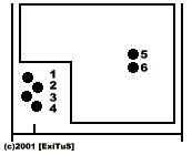
| Pin |
Signal |
| 1 |
Gnd |
| 2 |
FBus Tx |
| 3 |
MBus |
| 4 |
FBus Rx |
| 5 |
Vpp (Flash Progr. Voltage +12V) |
| 6 |
Vpp Gnd |

| Pin |
Signal |
| 1 |
WDDISX - Watchdog disable |
| 2 |
FBus Rx |
| 3 |
FBus Tx |
| 4 |
Vpp Gnd |
| 5 |
Gnd - Signal Gnd |
| 6 |
MBus - Serial clock from Prommer |
| 7 |
Vpp - Flash Programming voltage +12V |
| 8 |
Chrgr+ - Charger input |
Display Connector

| Pin |
Signal |
| 1 |
LCDRSTX - Reset (2,8V) |
| 2 |
VOUT - DC/DC voltage converter output (0V) |
| 3 |
Gnd (0V) |
| 4 |
LCDCSX - Chip select input (2,8V) |
| 5 |
LCDCDX - Control/display data flag input (2,8V) |
| 6 |
SDA - Serial data input (0V) |
| 7 |
SCLK - Serial clock input (0V) |
| 8 |
VBB - Suply voltage (2,8V) |

| Pin |
Signal |
| 1 |
Gnd (-) |
| 2 |
BTemp (Temperature) |
| 3 |
BSI (Battery Type / Capacity) |
| 4 |
VBatt (+) |
References
Category:Cellular
Phones Connectors


