
The side port is a 44-pin edge connector located on the right side of the Texas Instruments TI-99/4A home computer (introduced 1981). It exposes the complete TMS9900 CPU bus: a 16-bit address bus (A0–A15), an 8-bit bidirectional data bus (D0–D7), CRU serial I/O lines (CRUCLK*, CRUIN), and all memory control signals (MEMEN*, DBIN, WE*, READY). Additional signals include SBE (Speech Block Enable), IAQ (Instruction AcQuisition), EXTINT*, LOAD*, PHI3* (inverted CPU clock phase 3), and an AUDIOIN line routed to the sound generator. The connector’s pin assignment is fully tabulated in Section D.2.1 of the 1983 Texas Instruments document TI-99/4A Console and Peripheral Expansion System Technical Data (part no. 1049717-2). Sidecar peripherals such as the speech synthesiser and memory expansion units attached directly to this port; from 1982 onwards TI introduced the Peripheral Expansion Box (PEB), which connects via a cable to this port and presents a separate 60-pin backplane connector to internal expansion cards.
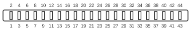
| Pin | Name | Dir | Description |
|---|---|---|---|
| 1 | VCC | - | +5 Volts power supply |
| 2 | SBE | OUT | Low if addr in >9000-94xx (sound port) |
| 3 | RESET* | OUT | System reset (active low) |
| 4 | EXTINT* | IN | External interrupt (active low) |
| 5 | A5 | OUT | Address bus, bit 5 |
| 6 | A10 | OUT | - |
| 7 | A4 | OUT | - |
| 8 | A11 | OUT | - |
| 9 | DBIN | OUT | Active high = read memory |
| 10 | A3 | OUT | - |
| 11 | A12 | OUT | - |
| 12 | READY | IN | Active high = memory is ready |
| 13 | LOAD* | IN | Unmaskable interrupt (=> BLWP @>FFFC) |
| 14 | A8 | OUT | - |
| 15 | A13 | OUT | - |
| 16 | A14 | OUT | - |
| 17 | A7 | OUT | - |
| 18 | A9 | OUT | - |
| 19 | A15 | OUT | Address bus, lsb. Also CRU output bit. |
| 20 | A2 | OUT | - |
| 21 | GND | - | Ground |
| 22 | CRUCLK* | OUT | Inversion of TMS9900 CRUCLOCK pin |
| 23 | GND | - | Ground |
| 24 | PHI3* | OUT | Inversion of phase 3 clock |
| 25 | GND | - | Ground |
| 26 | WE* | OUT | Write Enable (derived from TMS9900 WE* pin) |
| 27 | GND | - | Ground |
| 28 | MBE* | OUT | Active low if addr in >4000-5FFF (card ROMs) |
| 29 | A6 | OUT | - |
| 30 | A1 | OUT | - |
| 31 | A0 | OUT | Address bus, bit 0 (most significant) |
| 32 | MEMEN* | OUT | Memory access enable (active low) |
| 33 | CRUIN | IN | CRU input bit to TMS9900 |
| 34 | D7 | IN/OUT | Data bus, bit 7 (least significant) |
| 35 | D4 | IN/OUT | - |
| 36 | D6 | IN/OUT | - |
| 37 | D0 | IN/OUT | Data bus, bit 0 (most significant) |
| 38 | D5 | IN/OUT | - |
| 39 | D2 | IN/OUT | - |
| 40 | D1 | IN/OUT | - |
| 41 | IAQ | IN | Interrupt acknowledged by TMS9900 |
| 42 | D3 | IN/OUT | - |
| 43 | VDD | - | -5 Volts power supply |
| 44 | AUDIOIN | IN | To sound generator AUDIO IN pin |
Notes
The connector is a 44-pin edge connector with pins numbered 1–43 (odd) on the bottom edge and 2–44 (even) on the top edge. Power rails are +5 V at pin 1 (VCC) and −5 V at pin 43 (VDD); four ground pins (21, 23, 25, 27) are distributed across the connector. All address and control lines are driven by 74LS244 buffers; the data bus uses a bidirectional 74LS245 transceiver. The maximum capacitive load per signal line is 90 pF for D0–D7 and most control lines. Address lines must settle at least 100 ns before a memory access; DSR ROM access time must not exceed 650 ns. The MBE* signal is predecoded by the console to select the DSR ROM space (>4000–5FFF), making peripherals straightforward to decode without additional address logic. RESET* (pin 3) is active low and is system-driven. The PHI3* signal (pin 24) is the inverted phase-3 CPU clock and may be used by peripherals for synchronisation. The AUDIOIN line (pin 44) feeds directly into the console’s sound generator audio input.
Signals
- VCC — +5 V regulated power supply (pin 1)
- SBE — Speech Block Enable; driven low when the address bus is in the range >9000–94xx, indicating access to the speech synthesiser address block
- RESET* — Active-low system reset; console-driven
- EXTINT* — External interrupt input to the console; active low
- A0–A15 — 16-bit TMS9900 address bus; A0 is the most significant bit; A15 also carries the CRU output data bit during CRU output instructions
- DBIN — Data Bus IN; active high when the CPU is performing a memory read
- READY — Memory ready signal; active high indicates that the addressed device has data ready; peripherals pull this low to insert wait states
- LOAD* — Active-low unmaskable interrupt; triggers a BLWP (Branch and Link with Workspace Pointer) to the vector at >FFFC
- CRUCLK* — Inverted CRU clock output from the TMS9900; used for CRU (Communications Register Unit) serial I/O operations
- PHI3* — Inverted phase-3 CPU clock output; available to peripherals for timing
- WE* — Write Enable; derived from the TMS9900 WE* pin; active low during memory write cycles
- MBE* — Memory Block Enable; predecoded active-low select for the DSR ROM space >4000–5FFF; used by peripheral cards to enable their on-board DSR ROM without additional address decoding
- MEMEN* — Memory Enable; active low during any memory access cycle
- CRUIN — CRU serial input bit returned to the TMS9900 during CRU input instructions
- D0–D7 — 8-bit bidirectional data bus; D0 is the most significant bit
- IAQ — Instruction AcQuisition; high when the CPU is fetching an instruction opcode; available to peripherals for bus monitoring
- VDD — −5 V power supply (pin 43)
- AUDIOIN — Audio input routed to the console’s sound generator AUDIO IN pin; allows peripherals to mix audio into the console’s output