
EPP - Enhanced Parallel Port
The Enhanced Parallel Port (EPP) mode was jointly developed by Intel, Xircom, and Zenith Data Systems, first specified as EPP 1.7 in March 1992 and subsequently incorporated into the IEEE 1284-1994 standard governing bidirectional parallel peripheral interfaces for personal computers. EPP uses the same 25-pin DB-25 Type-A connector as the Standard Parallel Port (SPP) but reassigns the control and status lines to perform fully hardware-managed, bidirectional transfers at 500 KB/s to 2 MB/s — far exceeding the approximately 150 KB/s of Compatibility mode. Unlike ECP, which requires DMA and peripheral negotiation of a reverse channel, EPP generates all handshaking autonomously in hardware, making it well suited to scanner, storage, and networking peripherals that need high throughput with minimal firmware complexity. Two variants exist: EPP 1.7 (pre-standard) allows address and data strobes to assert without waiting for the nWAIT line to go low, whereas EPP 1.9 (IEEE 1284-compliant) requires nWAIT to be low before a cycle begins; both variants require nWAIT to go high before the cycle ends.
EPP Hardware Properties
When using EPP mode, a different set of signal names and functions are assigned to each line. It is common to see both the SPP and EPP names used interchangeably in parallel port data sheets and literature. All documentation here uses the EPP signal names.
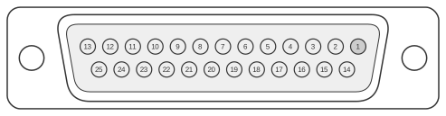 (25 PIN D-SUB FEMALE at the PC)
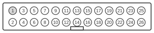 (26 Pin MALE connector on the mainboard)
| Pin | SPP Signal | EPP Signal | IN/OUT | Function |
|---|---|---|---|---|
| 1 | Strobe | Write | Out | A low on this line indicates a Write, High indicates a Read |
| 2 | data0 | data0 | IN/OUT | Address, Data or RLE Data Bit 0 |
| 3 | data1 | data1 | IN/OUT | Address, Data or RLE Data Bit 1 |
| 4 | data2 | data2 | IN/OUT | Address, Data or RLE Data Bit 2 |
| 5 | data3 | data3 | IN/OUT | Address, Data or RLE Data Bit 3 |
| 6 | data4 | data4 | IN/OUT | Address, Data or RLE Data Bit 4 |
| 7 | data5 | data5 | IN/OUT | Address, Data or RLE Data Bit 5 |
| 8 | data6 | data6 | IN/OUT | Address, Data or RLE Data Bit 6 |
| 9 | data7 | data7 | IN/OUT | Address, Data or RLE Data Bit 7 |
| 10 | Ack | Interrupt | In | Interrupt Line. Interrupt occurs on Positive (Rising) Edge. |
| 11 | Busy | Wait | In | Used for handshaking. A EPP cycle can be started when low, and finished when high. |
| 12 | Paper Out / End | Spare | In | Spare - Not Used in EPP Handshake |
| 13 | Select | Spare | In | Spare - Not Used in EPP Handshake |
| 14 | Auto Linefeed | Data Strobe | Out | When Low, indicates Data transfer |
| 15 | Error / Fault | Spare | In | Spare - Note used in EPP Handshake |
| 16 | Initialize | Reset | Out | Reset - Active Low |
| 17 | Select Printer | Address Strobe | Out | When low, indicates Address transfer |
| 18 | GND | GND | - | Signal Ground |
| 19 | GND | GND | - | Signal Ground |
| 20 | GND | GND | - | Signal Ground |
| 21 | GND | GND | - | Signal Ground |
| 22 | GND | GND | - | Signal Ground |
| 23 | GND | GND | - | Signal Ground |
| 24 | GND | GND | - | Signal Ground |
| 25 | GND | GND | - | Signal Ground |
Notes
- Direction is computer relative to device.
- Pins 12 (Paper Out/Spare), 13 (Select/Spare), and 15 (Error/Spare) are not defined in the EPP handshake and may be used freely by the application; their state is readable via the SPP Status Register at any time.
- The cable specification below (plug and conductor details) derives from the EPP Release 1.7 specification of March 1992; the IEEE 1284-2000 standard specifies a maximum cable length of 25 feet and a characteristic impedance of 62 ± 6 ohms.
- IEEE 1284 Level II drivers are required for reliable EPP operation: VOH ≥ 2.4 V at 14 mA source; VOL ≤ 0.4 V at 14 mA sink; output impedance 50 ± 5 ohms; slew rate 0.05–0.40 V/ns.
Signals
- nWrite (pin 1) — Active-low write indicator; low = write cycle, high = read cycle. Corresponds to SPP nSTROBE.
- AD0–AD7 (pins 2–9) — Bidirectional address/data bus. Carry the address during an address cycle and data during a data cycle.
- nINTR / Interrupt (pin 10) — Peripheral interrupt line; interrupt occurs on the rising (positive) edge. Corresponds to SPP nACK.
- nWAIT / Wait (pin 11) — Handshake signal driven by the peripheral; an EPP cycle may start when low and is complete when high. Corresponds to SPP BUSY.
- Spare (pin 12) — Not used in the EPP handshake. Corresponds to SPP Paper Out / PE.
- Spare (pin 13) — Not used in the EPP handshake. Corresponds to SPP SELECT.
- nDATASTB / Data Strobe (pin 14) — Active-low strobe indicating a data transfer cycle. Corresponds to SPP nAUTOFEED.
- Spare (pin 15) — Not used in the EPP handshake. Corresponds to SPP nERROR.
- nRESET / Reset (pin 16) — Active-low reset to the peripheral. Corresponds to SPP nINIT.
- nADDRSTB / Address Strobe (pin 17) — Active-low strobe indicating an address transfer cycle. Corresponds to SPP nSELECTIN.
- GND (pins 18–25) — Signal ground returns.
Cable specifications (EPP Release 1.7, March 1992)
Plug description
- DB25 Male, tin plated shell with indents, P.B.T. insulator, white color, 30µ° gold plated over 50µ° nickel, 4-40 thumbscrew hardware, molded with red color P.V.C.
- DB25 Female, tin plated shell, P.B.T. insulator, white color, gold flash over 50µ° nickel, 3/16 hex standoffs 1/4 inch long, threaded 4-40
Cable
- 28 AWG, tinned strande copper wire, UL2464 approved, foil shielded, gray color.
- Conductors:
- Inner layer: 8 wires with drain, aluminium foil and mylar shield.
- Outer layer: 8 twisted pairs, aluminium foil shield and jacket.
Both ends must be covered with aluminium foil shielding in a premolded connector hood.
References
- IEEE 1284-2000 — IEEE Standard Signaling Method for a Bidirectional Parallel Peripheral Interface for Personal Computers
- IEEE 1284-1994 — IEEE Standard Signaling Method for a Bidirectional Parallel Peripheral Interface for Personal Computers (superseded)
- IEEE 1284 EPP Mode — Signal Mapping and Register Interface
- IEEE 1284-1994 Standard — MCABase Technical Reference